A future quantum computer may need millions of qubits working together. Most current chips struggle with a much smaller problem.
Their qubits can usually communicate only with nearby neighbors. That short reach creates a serious obstacle. A useful processor must coordinate information across an entire chip without filling it with bulky connecting hardware.
Researchers at the University of Warwick and NRC Canada have proposed a different route. Their concept uses tiny sound-like vibrations to carry quantum information between distant qubits.
They call the system Quantum Phononic Links, or QPLs.
It combines a new chip architecture with compressively strained germanium grown on silicon. In principle, the links could connect qubits sitting beside each other or separated across a 300-millimeter semiconductor wafer.
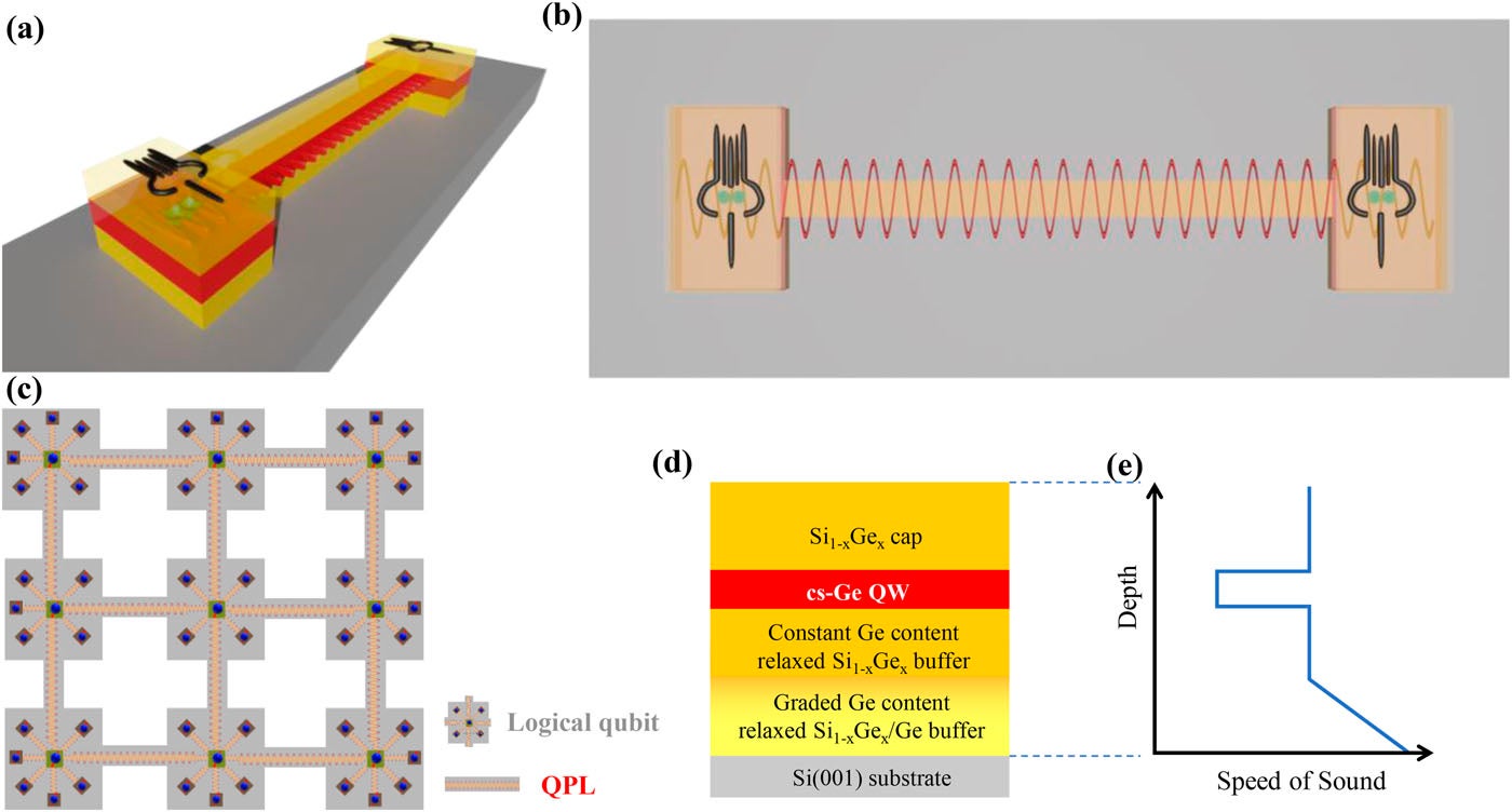
“One of the key challenges in quantum computing is long-range qubit connectivity,” said Dr. Maksym Myronov of Warwick’s Department of Physics.
“Our work introduces a new concept in which phonons act as a quantum bus, enabling distant qubits to exchange quantum information while remaining fully compatible with semiconductor technology.”
Quantum computers store and process information using qubits. Building larger machines requires those qubits to interact in controlled ways.
Many leading designs rely on short-range coupling. That arrangement works best when the qubits sit extremely close together. The problem grows with the chip.
A processor containing hundreds of thousands or millions of qubits cannot depend only on local connections. Information must travel between distant areas without disrupting nearby operations.
Several possible solutions already exist. Some use microwave resonators. Others move charge or generate surface acoustic waves outside the qubit material.
Those methods can require extra components, large structures, or difficult fabrication steps.
Quantum Phononic Links take another approach. Instead of sending information through electromagnetic signals, they use phonons. These are organized vibrations moving through a material.
The phonons act like a communication channel built into the same semiconductor layer that hosts the qubits.
That makes the system a material-native quantum bus.
The proposed architecture uses hole spin qubits in compressively strained germanium on silicon.
Warwick researchers have developed this material through advanced epitaxial growth methods. It consists of a thin germanium crystal layer formed within a silicon-based structure. The qubits respond strongly to small deformations in that layer.
When a phonon passes through the crystal, it creates a changing strain field. That strain alters the electronic conditions surrounding the hole spins.
The interaction allows the vibration to affect a qubit directly. No separate piezoelectric transducer is required.
That distinction matters because piezoelectric layers can complicate manufacturing. They may also introduce electric fields and noise that weaken quantum performance.
Direct strain coupling keeps the system within the semiconductor platform.
The researchers describe operation at frequencies reaching many gigahertz. These high frequencies also help reduce unwanted thermal vibrations at very low temperatures.
Quantum processors commonly operate inside dilution refrigerators. The study considers temperatures between about 10 and 100 millikelvin.
At 100 millikelvin, thermal energy reaches about 8.6 microelectronvolts. A 10-gigahertz phonon carries roughly 40 microelectronvolts.
That gap helps suppress random thermal phonons. The intended vibrations should therefore stand out more clearly from the background.
The germanium layer serves two roles.
It hosts the hole spin qubits. It also guides the vibrations carrying information between them. The surrounding silicon-germanium layers act as acoustic cladding, much like the outer layer around an optical fiber.
Differences in sound speed create an acoustic contrast of roughly 10% to 20%. That contrast can confine phonons within the germanium region.
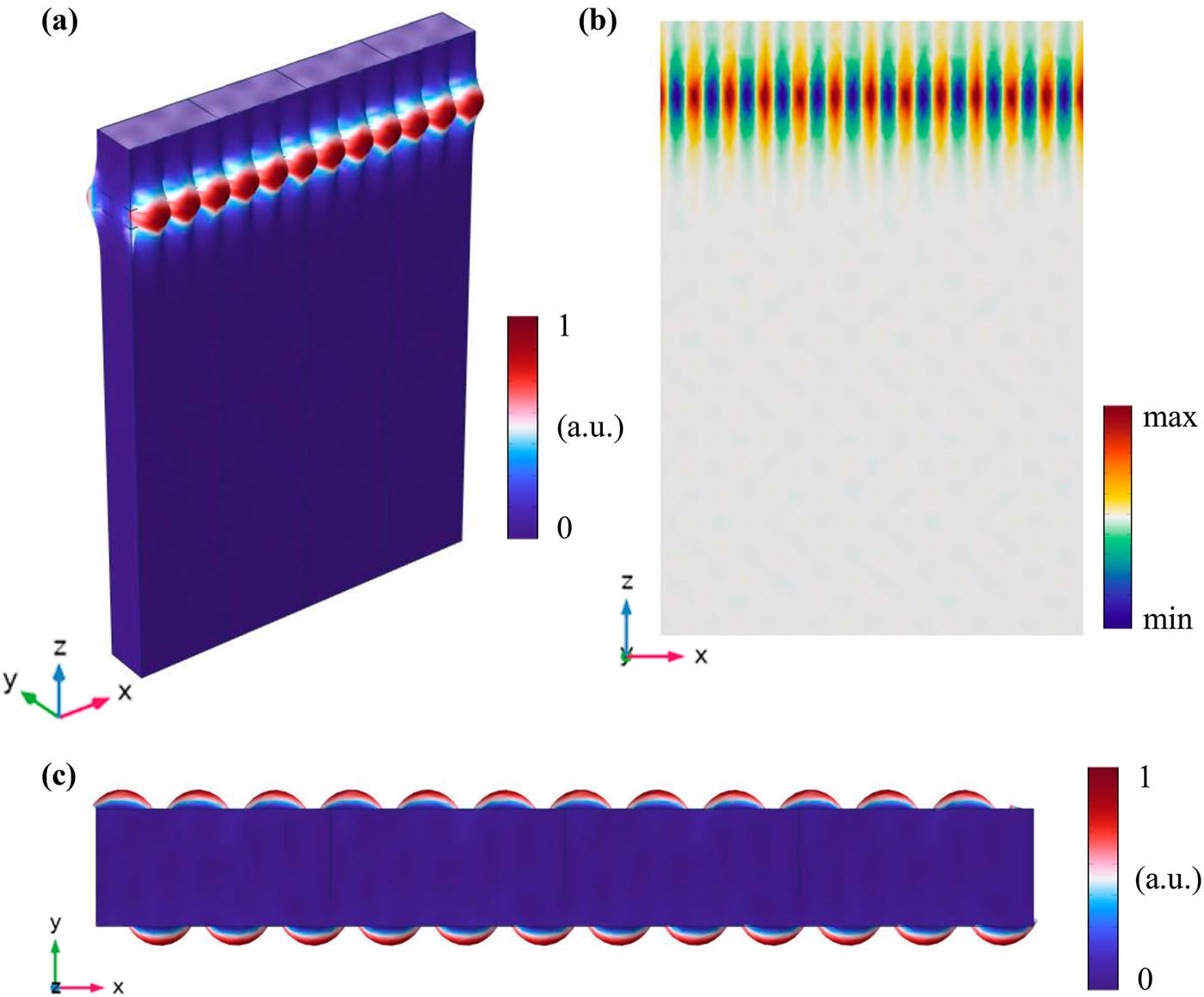
Computer simulations indicated strong localization inside the quantum well.
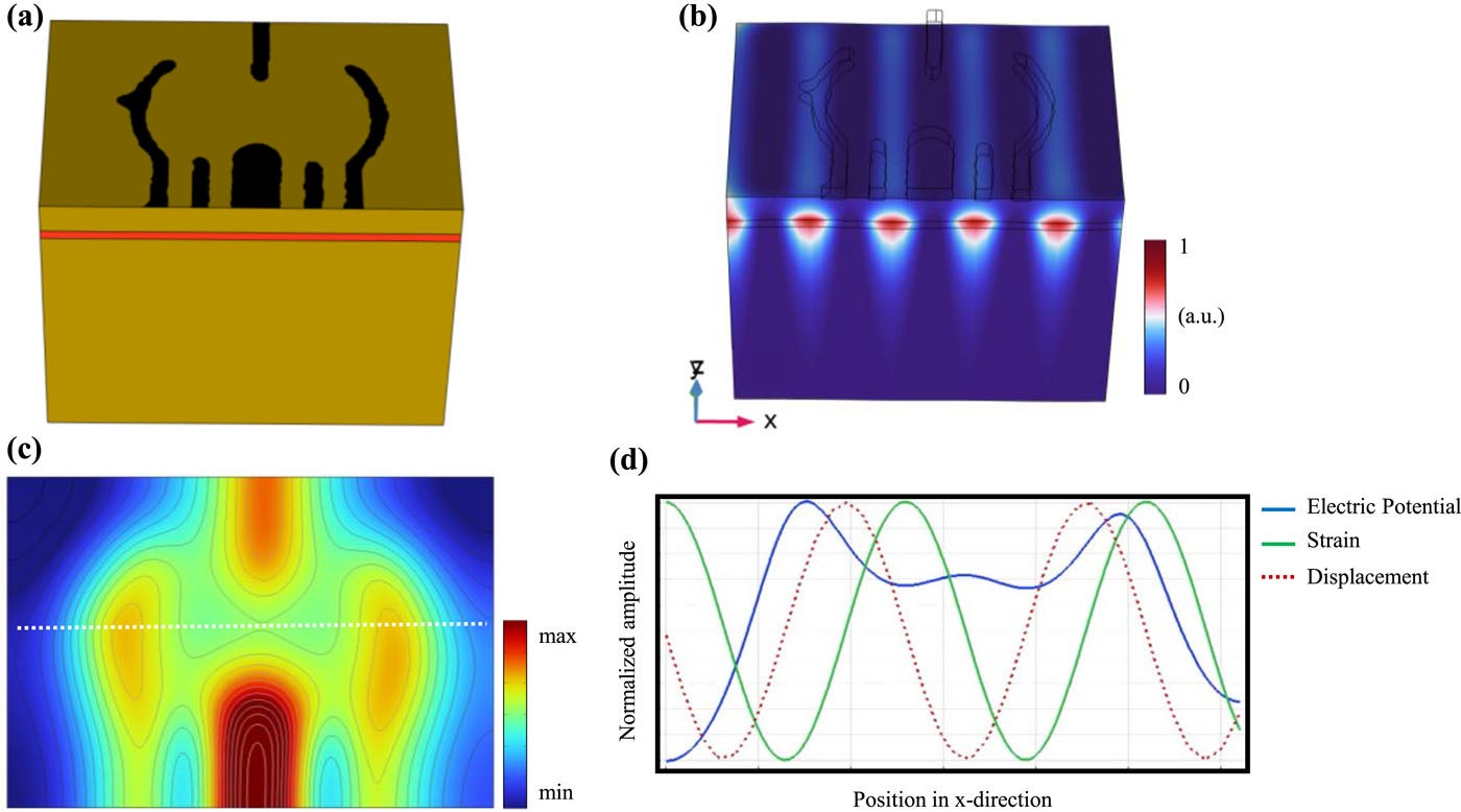
At a simulated frequency of 50 gigahertz, the phonon displacement remained concentrated where the qubits would sit.
The associated strain field also overlapped with those locations. Researchers found that spacing two quantum dots by half a phonon wavelength could strengthen the interaction.
One dot would sit near a strain maximum. The other would lie near a minimum. That arrangement creates a 180-degree phase difference and increases the modulation of the qubit energy levels.
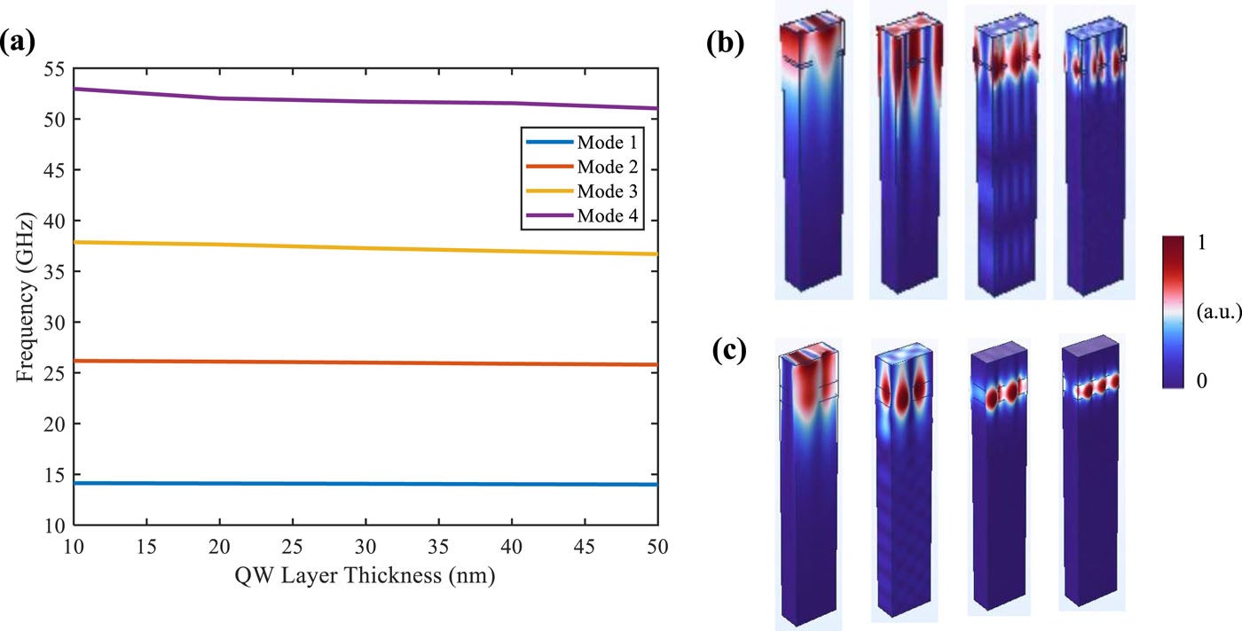
Engineers could adjust several features to tune the link. These include the germanium thickness, the level of strain, the surrounding material, and the shape of waveguides or cavities.
Each choice affects how the phonons travel, where they remain confined, and how long they persist.
The chip would not simply contain a straight acoustic path. It could include channels, storage regions, and frequency-selective structures.
Sound travels much more slowly than light. That slower speed gives gigahertz phonons wavelengths measured in hundreds of nanometers. Microwave systems operating at similar frequencies can require far larger structures.
The smaller scale could help preserve valuable chip space.
Quantum Phononic Links might connect components less than one micrometer apart. The same principle could extend across much larger sections of a wafer.
The press release describes possible communication across a chip up to 300 millimeters wide. Real devices would still face losses.
Interface roughness, alloy disorder, and defects can scatter phonons or shorten their coherence. The researchers estimate that coherent travel could remain practical over tens of micrometers to several centimeters.
Improved fabrication and phononic band engineering might allow longer links.
Band engineering could also block unwanted vibrations while guiding selected modes.
Cavities could hold acoustic energy temporarily. That storage would give phonons more time to interact with spin qubits. The system could then operate as either a shared connection or a traveling messenger.
In one proposed mode, several qubits would connect through a common phononic cavity. The shared vibration could help distant qubits interact or become entangled.
A second mode would use individual phonons moving through waveguides.
These traveling phonons would carry quantum information much like photons move through optical communication systems. The researchers estimate single-phonon spin coupling strengths between about 0.1 and 10 megahertz.
The exact value would depend on confinement, device geometry, and overlap with the qubit.
They also considered quality factors between 10,000 and 1 million. Assumed spin coherence times ranged from roughly 1 to 10 microseconds.
Under some of those conditions, the calculated cooperativity could reach or exceed one. That result suggests coherent spin-phonon interactions may be possible.
The coupling could also be switched electrically.
By changing voltages on gate-defined double quantum dots, engineers might turn the interaction on or off within about one nanosecond. Fast control would support pulsed operations across the chip.
The paper also outlines a method for detecting a single phonon. A double quantum dot could enter a metastable latching state.
Absorbing a phonon would trigger a charge change. That state would last long enough for a standard charge sensor to record it. Such detection could support future protocols that confirm when a quantum signal has arrived.
Quantum Phononic Links remain a proposed architecture. The study presents modeling, design principles, and expected performance. It does not report a complete processor using the links.
Fabrication quality will shape what distances become realistic. Phonon losses and defects remain important engineering limits.
Large quantum machines would also require many systems beyond connectivity.
Still, the concept targets a specific barrier that grows as chips become larger. Because the links use semiconductor materials and lithographic design, they could fit existing manufacturing methods more easily than some external systems.
The work extends Warwick’s research on strained germanium materials. It also continues the university’s semiconductor partnership with NRC Canada.
The UK Engineering and Physical Sciences Research Council supported the research. NRC Canada’s Quantum Sensing Program also provided support.
The design could give engineers more freedom when arranging qubits.
They would not need every interacting pair to sit directly beside each other. That may reduce crowding and simplify large processor layouts.
A built-in phonon network could also limit the need for separate microwave structures or acoustic hardware. Smaller connections may leave more chip area available for qubits, controls, and readout systems.
The same platform could support several connection lengths and frequencies. Engineers could shape those properties during fabrication.
Future experiments must confirm whether the modeled links preserve quantum information under realistic conditions. Researchers will also need to measure losses, fabrication tolerances, and control accuracy across larger devices.
The proposal does not solve every problem facing million-qubit machines.
It does, however, offer a compact answer to one of the hardest questions: how distant qubits on the same chip might speak to each other.
Research findings are available online in the journal APL Quantum.
The original story “New quantum chip design uses phonons to link distant qubits” is published in The Brighter Side of News.
Like these kind of feel good stories? Get The Brighter Side of News’ newsletter.
The post New quantum chip design uses phonons to link distant qubits appeared first on The Brighter Side of News.

