The surface of diamond may hold a hidden electrical advantage that could shape future electronics. Researchers at the University of Electro-Communications have developed a new way to map how materials respond to electric fields in three dimensions, down to the atomic scale. Using that method, they found that diamond-like carbon films behave in a surprising way near their surface.
Most materials lose some dielectric strength at their outer edge. Silicon, the material used in many computer chips, follows that pattern. But hydrogen-terminated diamond-like carbon showed the opposite effect. Its surface response increased beyond the value expected from bulk diamond.
That unexpected boost came from unusual surface electrons. These electrons behave almost as if they are floating near the material, making them highly responsive to electric fields.
Modern electronics depend on materials that can store, manage and control electrical energy. Smartphones, sensors, medical devices and computer chips all rely on these properties.
As devices shrink, surfaces matter more. In a thick material, most atoms sit safely inside. In a thin film, many atoms sit near an edge or interface. That means surface behavior can shape the whole device.
A key property is the dielectric constant. It measures how strongly a material responds to an electric field. Higher local dielectric response can improve how materials store and handle electrical energy.
Until now, scientists struggled to see this response in full three-dimensional detail at the atomic level. Bulk measurements often hide what happens across just one or two layers of atoms.
The research team built a method to visualize local dielectric behavior in three dimensions. This allowed them to see where a material responded strongly or weakly to an electric field.
The team used first-principles calculations, which model material behavior from basic quantum rules. They studied thin films of hydrogenated carbon and hydrogenated silicon.
These films are written as C(111)-H and Si(111)-H. Both have hydrogen atoms attached to their surfaces. Their structures are similar enough to compare directly, but their electrons behave differently.
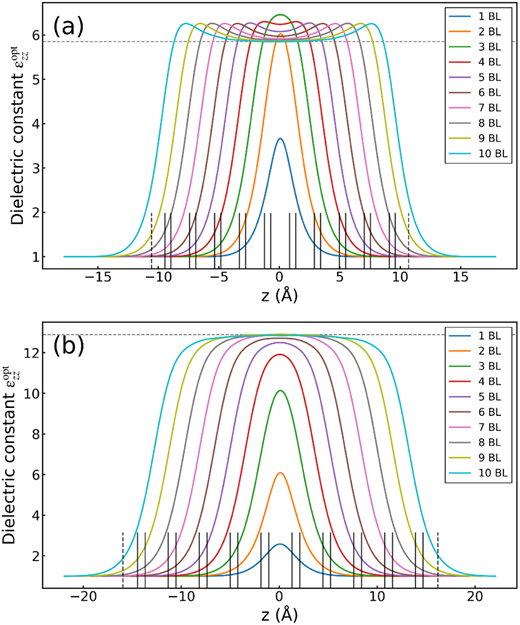
The researchers created models from one to 10 bilayers thick. They then applied electric fields and calculated how charges shifted inside and near each film.
From those charge shifts, they built atomic-scale maps of the dielectric constant.
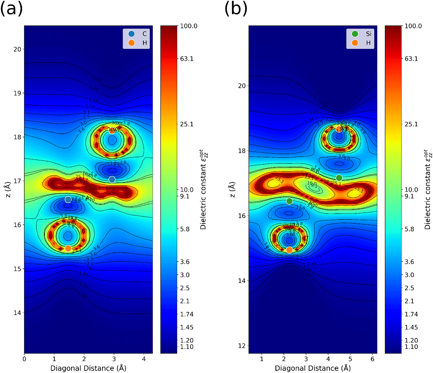
The silicon film behaved as researchers expected. Near the surface, its dielectric constant decreased. This matches earlier studies of Si(111)-H films.
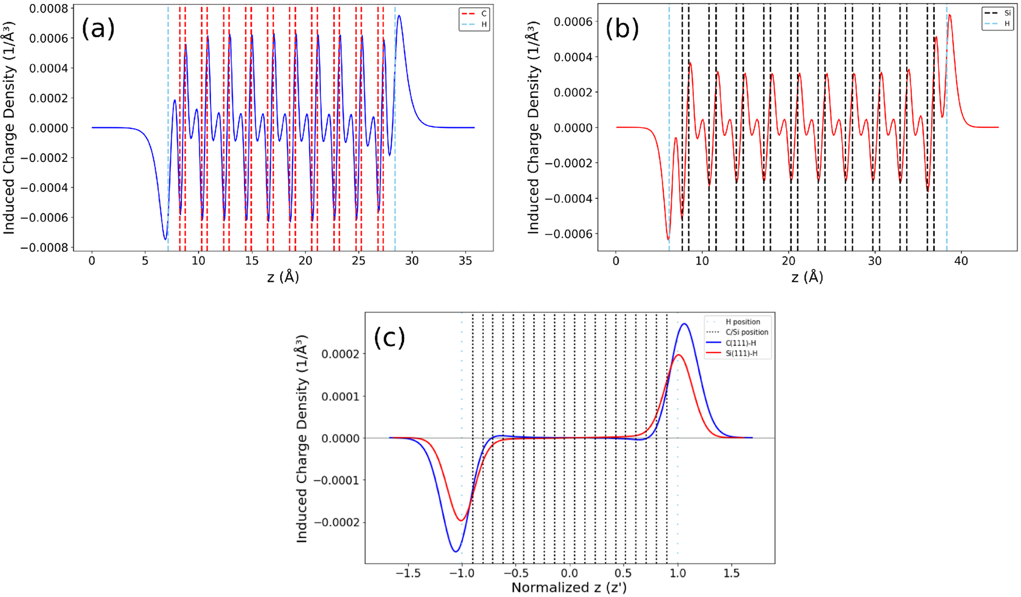
In silicon, induced charge spreads several layers into the film. This reduces the surface’s ability to respond strongly to the electric field.
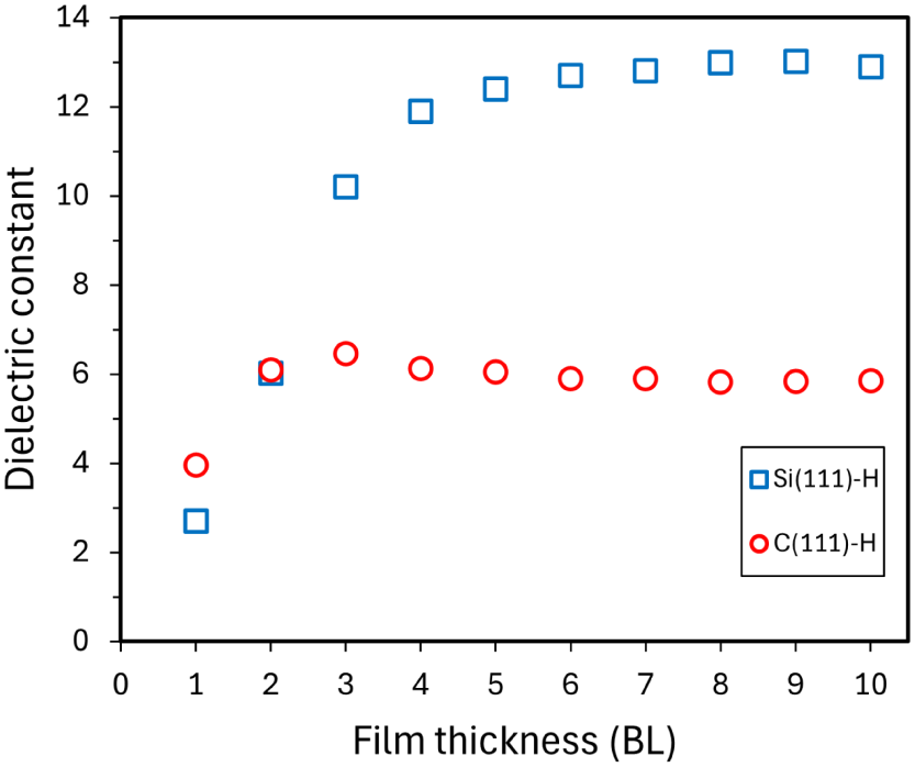
As the silicon films became thicker, the center of the film behaved more like bulk silicon. Its dielectric value rose steadily toward the known bulk value.
This result gave the team an important reference point. Their method reproduced the expected behavior for a familiar material.
Then diamond-like carbon surprised them.
The carbon film showed a very different surface response. Instead of losing dielectric strength near the surface, it gained it.
In the region about one to two bilayers from the surface, the dielectric constant rose above the bulk diamond value. This was unexpected because bulk diamond has a lower dielectric constant than bulk silicon.
The charge response also looked different. In silicon, the induced charge appeared above the outer hydrogen atoms. In carbon, the charge shifted outward, toward the vacuum beyond the surface.
That outward shift offered a clue. Something near the diamond-like surface was responding strongly to the electric field.
The researchers traced the effect to a nearly free electron state.
A nearly free electron state is an unusual electronic state that extends beyond a material’s surface. In simple terms, part of the electron’s behavior reaches outward instead of staying tightly inside the solid.
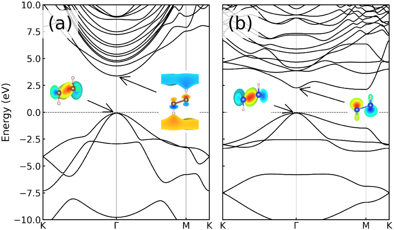
In the carbon film, this state formed the conduction band minimum. That means it was the lowest available energy state for excited electrons.
Because the state sits at this important energy level, it plays a major role in how the material responds to electric fields.
These electrons are weakly bound near the surface. They can shift more easily when an electric field appears. That makes them highly polarizable.
This high polarizability boosts the local dielectric constant near the carbon surface.
Both carbon and silicon films can have nearly free electron states. But their energy positions differ.
In C(111)-H, the nearly free electron state sits at the conduction band minimum. In Si(111)-H, it lies above that level. That difference changes how strongly the state affects electric response.
The researchers examined electronic band structures to confirm this. In silicon, the key conduction state looked like a silicon-silicon antibonding orbital. It did not show the same nearly free character.
In carbon, the lowest conduction state spread broadly from the surface into the vacuum. Its location matched the region where the dielectric response increased.
That link gave the study its central message. Surface electronic states can control local dielectric behavior.
The team also tested the idea using a cubic boron nitride thin film. This helped show that the effect was not limited to carbon.
In that material, a nearly free electron state appeared only on the nitrogen side. The dielectric enhancement also appeared only on that side.
The boron side did not show the same increase. This supported the conclusion that the nearly free electron state drives the surface boost.
The researchers still describe the connection as mainly qualitative. More work will be needed to measure exactly how much the state contributes.
Future studies may examine different surface treatments, electron masses and surface shapes.
The findings matter because electronics keep moving toward thinner and smaller structures. In that world, local surface effects can no longer be ignored.
A material’s bulk value may not tell the full story. A surface, interface or special electronic state can change how the device behaves.
For carbon-based technologies, this could be especially useful. Hydrogenated diamond surfaces already interest researchers because they can have negative electron affinity. That means electrons can leave the surface more easily under the right conditions.
When combined with nearly free electron states, this feature may help create efficient electron sources. One possible application is cold cathodes, which can emit electrons at low voltages.
Such devices could support faster, cooler and more energy-efficient electronics.
The study does not claim that diamond-based devices are ready for everyday use. It offers something more basic but powerful: a clearer map of how surfaces behave.
Engineers need this kind of knowledge to design future materials. As films reach atomic thickness, small surface changes can have large effects.
The new mapping method gives researchers a way to see those changes directly. It can connect local dielectric behavior with specific electronic states.
That makes it useful beyond diamond and silicon. It could help study insulators, thin films, two-dimensional materials and nanoscale device structures.
This research could help engineers design smaller and more efficient electronic components. By mapping dielectric response in three dimensions, scientists can identify where materials handle electric fields best. That matters as devices shrink to scales where surface atoms strongly affect performance.
The discovery may be especially important for carbon-based technologies. Hydrogenated diamond-like films showed an enhanced surface response because of nearly free electrons. If researchers learn to control this effect, they could build devices that use less energy and stay cooler.
The work may also support future cold cathodes. These electron sources could operate at lower voltages while producing dense electron flow. That could benefit advanced electronics, sensors and other technologies that need controlled electron emission.
More broadly, the study shows that surfaces can create properties not seen inside bulk materials. This insight gives researchers a new path for designing materials from the atomic level up. It may help future gadgets become faster, smaller and more energy efficient.
These resources explore hydrogen-terminated diamond, atomic-scale surface structure, electron emission and the growing use of diamond in next-generation electronic devices.
In-Substrate Imaging of Diamond–hBN FET Current via Wide-Field Quantum Diamond Microscopy
Researchers directly mapped current flowing through hydrogen-terminated diamond field-effect transistors, showing how defects and interfaces can create uneven electrical behavior inside working devices. (ACS Applied Electronic Materials, 2026)
Structural and electronic properties of hydrogen-terminated diamond field-effect transistors with h-BN gate dielectric featuring native point defects
First-principles calculations show how defects in a boron nitride gate dielectric alter electronic bands at a hydrogen-terminated diamond interface, highlighting how atomic-scale surface conditions can affect transistor performance. (Applied Physics Letters, 2025)
Emission properties of a hybrid metallized diamond(001) photocathode
This experimental work examines electron emission from diamond and reports emission involving conduction bands associated with both positive and negative electron affinity, directly connecting diamond’s surface electronic structure with its potential as an electron source. (Physical Review Accelerators and Beams, 2025)
Atomic Observation on Diamond (001) Surfaces with Near-Contact Atomic Force Microscopy
Researchers achieved atomic-resolution imaging of diamond surfaces and combined the measurements with density-functional calculations, providing a detailed view of surface carbon structures important for understanding diamond behavior at nanoscale dimensions. (Nano Letters, 2025)
Diamond: Recent Progress in Synthesis and Its Potential in Electronics
This broad review examines advances in diamond growth, electronic properties and device applications, providing useful context for why diamond is being investigated as a material for future high-performance electronics. (Chemistry of Materials, 2025)
Research findings are available online in the journal ACS Omega.
The original story “Diamond surface electrons could power smaller, cooler electronics” is published in The Brighter Side of News.
Like these kind of feel good stories? Get The Brighter Side of News’ newsletter.
The post Diamond surface electrons could power smaller, cooler electronics appeared first on The Brighter Side of News.


Leave a comment
You must be logged in to post a comment.